Everything you need to know about Printed Circuit Board
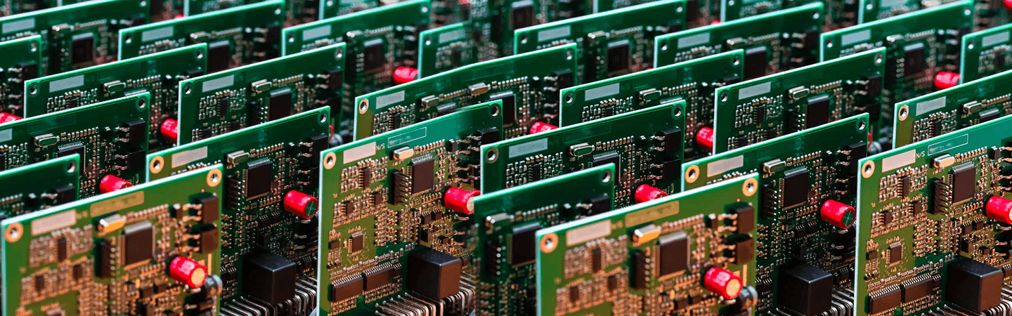
Definition of PCB – A printed circuit board popularly known as PCB is an electronic circuit that is used in the device to provide a pathway to its electronic components and mechanical support. PCBs are used in both laptop and desktop computers, they are used in internal computer components such as expansion cards, network interface cards, controller cards, and video cards. All the components connect to the motherboard that is also a printed circuit board.
Besides PCs, PCBs are used in many electronic devices. Most digital cameras, TVs, digital cameras, tablets, and cellphones include one or more PCBs.
Pcb full form in study
In the year 1936, Austrian engineer, Paul Eisler while he was working in the united kingdom invented the printed circuit.
Features of PCB
- The high density of PCB can be developed with the enhancement and progress of installation technology and integrated circuit
- A series of tests, inspections will ensure that the printed circuit board will work for a longer period.
- Regarding various properties, requirements (mechanical, physical, chemical and electrical, etc) of printed circuit boards can be reached through standardization and normalization of design with high efficiency and short span of time.
- A complete standard and various test instruments and equipment were established to evaluate and test the PCB products service and qualification life
- PCB products are not only automated but also can facilitate the standardized assembly of multiple components.
- Various components and PCB can be well assembled into larger systems, whole machines, and components
- As printed circuit boards components and products are assembled into the parts that are manufactured and designed in a standardized way.
How are Printed Circuit Boards Made?
PCBs are made with copper. The copper is plated to a substrate and carved to explode the specific design of the board. As there are many layers, they are lined up and integrated for a secure fit.
PCB manufacturers have focused on making PCBs durable, small, and able to include electrical power. PCBs now have evolved to be used as everyday electrical consumer products.
Pcb board material – PCBs use a variety of materials such as components and substrates. The selection of the material depends on the material requirements as different material choices will provide circuits of varying qualities that enable performance in specific circumstances.
Designers often choose materials that are based on electrical performance for high thermal survivability, high-speed applications, or mechanical for instance automotive under the hood applications.
PCB designers face several types of performance features when they focus on the material selection for their respective designs. Some of the popular considerations include
- Mitigated loss factors
- Flame retardance
- Dielectric constant
- Thermal performance
- Dimensional stability
Pcb layout design – There was one default trace clearance and width rule to set. Designers are responsible for manually changing the respective
width for ground and power nets, controlled any other net requirements. Designers either manipulate the grid or reset the value and draw spacings
around the layer in the part of the graphical for the visual reference for companies that require more clearances than the default value.
It is vital to make sure that rules which are entered into the schematic transfer over specifically and correctly into the respective layout. Adding rules which weren’t included initially in the schematic often happens with power.
Adding the manufacturing and mechanical clearance rules.
The different types of PCBs available are
- Rigid PCBs
- Flex PCBs
- Double-Sided PCBs
- Single-Sided PCBs
- Rigid-Flex PCBs
- Multilayer PCBs
How are PCBs Made?
PCB’s were made out of only one-sided capabilities and cardboard. There are many fabrication techniques that will make design evolve from a virtual image on your computer system to the tangible. There are four layers of PCB designs that include solder mask, substrate, copper, and silkscreen. All together must be aligned for the final product to become active. After designing a PCB and sending your PCB design off to the respective manufacturers and for starters they tend to use the design of your PCB as the blueprint for the whole process. Most often Through-Hole Method, Creating Layers, Surface Mount Technology, and Simple As a Stencil.
Pcb layers
In printed circuit boards you can select to cater as per the needs of your product from single-sided boards to flexible boards. In each of these circuit boards, there are a number of layers that contribute to their functionality.
Substrate Layer – It is made from fiberglass that gives the rigid form and can be also made with materials such as epoxies
Copper Layer – This is useful in many electronic products as the circuits on one side of the board as can be well connected to the other with holes that are drilled into it
Solder Mask Layer – The solder Mask layer is vital for the manufacturing process where the components are well soldered onto the board.
Silkscreen Layer – The silkscreen is for the purpose to understand the board of different pins or LEDs by adding numbers, letters, and symbols to the board.
Avench is one of the leading embedded IoT systems and embedded companies in the United States. For any sales queries, wait for no further contact us at +1 (775) 404-5757. You can also email us at sales@avench.com, we will be happy to assist you.