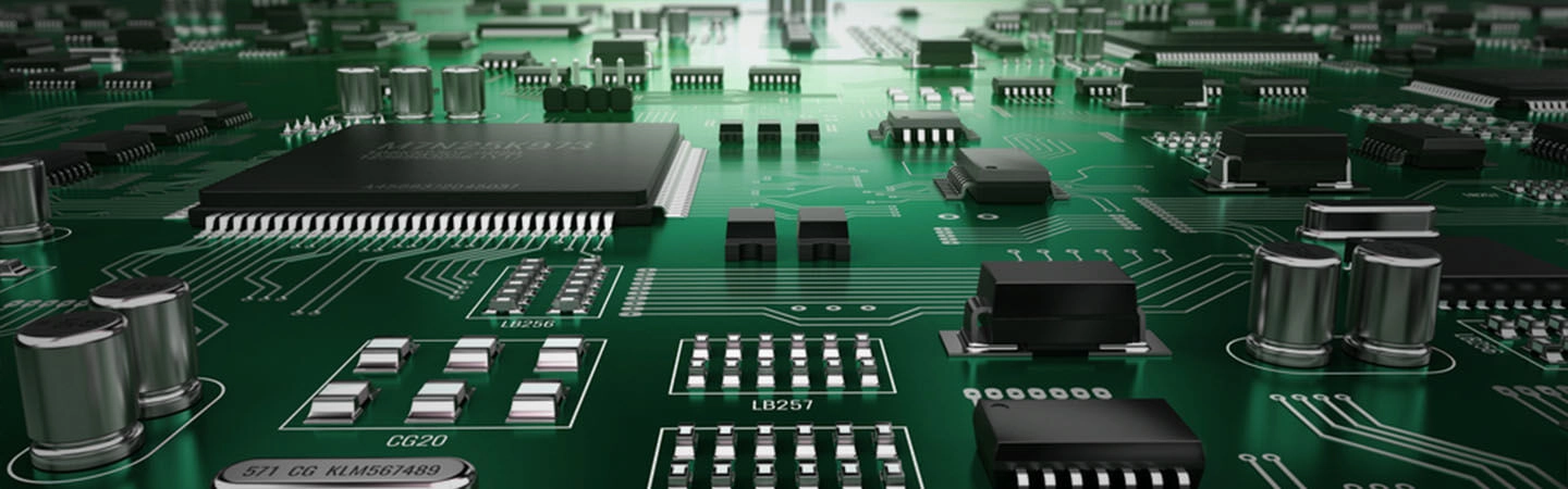
The Art of Designing A PCB Layout
Overview of PCB Design
The primary step involved in pcb layout design is creating concept block diagrams using a tool of your preference. The block diagram is then developed into schematic designs. An ideal schematic consists of net connections between symbols and component symbols. On the circuit board, the nets will then become the traces.
Pre-layout is the next stage of design, in which Bill of Materials (BOM) from the schematic is validated for obsolete components and long lead time components. During the process of validation, the vendor part numbers and manufacturing part numbers (MPN) are verified. The stack-up design is also completed during this stage.
Next is the PCB layout stage, in which the board outline, board parameter settings, component placement, production document generation and routing are accomplished.

The basic steps of PCB design:
The design process includes various stages. Each stage has its own checklists and defined processes. It is vital to follow a checklist at every milestone. Further we will discuss the different steps that are involved in designing a PCB.
Step 1: PCB schematic creation
A schematic diagram is a reflection of the elements of a system using graphic symbols and abstract. In this pcb schematic creation phase, the design is entered into a schematic tool (Allegro, Altium etc). A schematic reflects the components which are used in the design and how they are connected with each other. The schematic may define the relationships between the groups of components in various schematics. Schematic generation is all about the process of creating a logical representation of an electronic circuit. When you connect a collection of components in a unique way by creating a unique electronic product, you tend to generate a schematic.
Step 2: Pre-layout stage
In this pre-layout stage, by ensuring the BOM is verified for all the parts, the design of stack-up is initiated and verified that the parts are not obsolete and active.
BOM (Bill of Materials) validation –
For the purpose of manufacturing a printed circuit board, BOM is a list of required PCB materials. The primary step in this stage is to ensure that required materials for the purpose of design are available.
The following items are verified, during the BOM validation.
- To ensure manufacturing part numbers (MPN) are correct
- To ensure vendor part numbers (VPN) are correct
- To ensure the quantity of the parts is correct
- To ensure DNI (Do Not Install) components are marked in BOM
- To ensure designators match the schematic
Step 3: PCB layout stage
At this layout stage following activities are taken up – setting up the board outline, design tools, component placement, import of netlist, silkscreen cleanup, routing, generation of documents for products (netlist, gerbersetc) and DRC check.
Setting up the stack-up
The board layout is started by setting the design rules and stack-up. By using the layer stack-up manager tool, the stack-up is set up in the tool. The stack-up design that is generated from the PCB manufacturer is used as a reference to set it up in the layout tool.
Step 4: Generate the production lines
Gerbers and other production files are generated such as Topper copper layer(TCP), Solder mask top layer(SMT), Solder paste top layer (SPT), SilkScreen Top (SST), Bottom copper layer(BOT), Solder mask bottom layer (SMB), Solder paste bottom (SPB), Silk screen botto (SSB) and Inner layers signal and power/GND.
Perform a DFM check
Design for manufacturing (DFM) is all about a set of design guidelines that helps in verifying the manufacturability of design. During assembly and fabrication, DFM analysis identifies the PCB layout issues that may create any manufacturing problems.
The main factors that are to be considered while choosing a PCB design software include:
- Large components libraries
- Features
- User interface (UI)
Avench is one of the leading embedded companies in the United States.
To know more information about embedded product design and embedded systems please subscribe to our blog. For any sales queries, contact us at +1 (775) 404-5757. You can also email us at sales@avench.com – we would be happy to assist you.